Introduction
General Product Information
The RT8008 is a high-efficiency pulse-width-modulated (PWM) step-down DC/DC converter. Capable of delivering 600mA output current over an input voltage range of 2.5V to 5.5V, the RT8008 is ideally suited for portable electronic devices that are powered from 1-cell Li-ion battery (or from other power sources within that range) such as cellular phones, PDAs and handy-terminals.
An internal synchronous rectifier with low RDS(ON) dramatically reduces conduction losses in PWM mode. No external Schottky diode is required in practical applications. The RT8008 automatically turns off the synchronous rectifier when the inductor current is low entering discontinuous PFM mode to increase efficiency at light loads.
The RT8008 enters Low-Dropout mode when normal PWM operation cannot regulate the output voltage, turning on the upper P-MOSFET continuously. The RT8008 enters shutdown mode and consumes less than 0.1μA when EN pin is pulled low.
The switching ripple is easily smoothed-out by small sized filtering elements due to a fixed operating frequency of 1.5MHz. This, along with its small SOT-23-5 and TSOT-23-5 packages provides a small PCB area. Other features include soft start, low internal reference voltage with 2% accuracy, over temperature protection, and over current protection.
Product Feature
- 2.5V to 5.5V Input Range
- Adjustable Output from 0.6V to VIN
- 1.0V, 1.2V, 1.5V, 1.8V, 2.5V and 3.3V Fixed/ Adjustable Output Voltage
- 600mA Output Current, 1A Peak Current
- 95% Efficiency
- No Schottky Diode Required
- 1.5MHz Fixed Frequency at PWM Operation
- Small SOT-23-5 and TSOT-23-5 Package
- RoHS Compliant and 100% Lead (Pb)-Free
Key Performance Summary Table
|
Key features
|
Evaluation board number: PCB003_V1
|
|
Default Input Voltage
|
5V
|
|
Max Output Current
|
600mA
|
|
Default Output Voltage
|
1.2V
|
|
Default Marking & Package Type
|
RT8008GB, SOT-23-5
|
|
Operation Frequency
|
Steady 1.5MHz at PWM
|
|
Other Key Features
|
PSM/ PWM Auto Switched.
|
|
Protection
|
Over Current Protection, Over Temperature Protection
|
Bench Test Setup Conditions
Headers Description and Placement
Please carefully inspect the EVB IC and external components, comparing them to the following Bill of Materials, to ensure that all components are installed and undamaged. If any components are missing or damaged during transportation, please contact the distributor or send e-mail to evb_service@richtek.com.
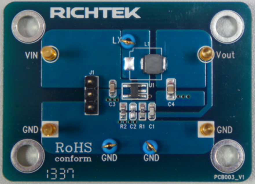
Test Points
The EVB is provided with the test points and pin names listed in the table below.
|
Test point/
Pin name
|
Signal
|
Comment (expected waveforms or voltage levels on test points)
|
|
VIN
|
Input voltage
|
Input voltage range= 2.5V to 5.5V
|
|
VOUT
|
Output voltage
|
Default Output Voltage = 1.2V
Output voltage range= 0.6V to 5V
(see ‘’ Output Voltage Setting’’ section for changing output voltage level)
|
|
LX
|
Switching node test point
|
LX waveform
|
|
J1
|
Chip Enable control
|
Drive EN or install a shorting block on Jumper J1 to enable operation (shorting 1-2) or disable operation (shorting 2-3).
|
|
GND
|
Ground
|
Ground
|
Power-up & Measurement
Procedure
1.Apply a 5V nominal input power supply (2.5V < VIN < 5.5V) to the VIN and GND terminals.
2.Place a shorting block across pins 1 and 2 of the J1 jumper to connect EN to VIN (>1.5V), to turn on the converter. Short pins 2-3, connecting EN to GND, to turn off the converter.
3.Verify the output voltage (approximately 1.2V) between VOUT and GND.
4.Connect an external load up to 600mA to the VOUT and GND terminals and verify the output voltage and current.
Output Voltage Setting
Set the output voltage with the resistive divider (R1, R2) between VOUT and GND with the midpoint connected to FB. The output is set by the following formula:

The installed VOUT capacitor (C4) is a 10μF, 6.3V X5R ceramic type. For higher output voltages, consider its voltage coefficient (capacitance vs. bias voltage) and ensure that the capacitance is sufficient to maintain stability and provide sufficient transient response for your application. This can be verified by checking the output transient response as described in the RT8008 IC datasheet.
Schematic, Bill of Materials and Board Layout
EVB Schematic Diagram
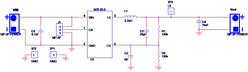
C3: 4.7μF/6.3V/X5R, 0603, TDK C2012X5R0J475M
C4: 10μF/6.3V/X5R, 0805, TDK C2012X5R0J106M
L1: 2.2μH TAIYO YUDEN NR3015T2R2M, DCR=60mΩ
Bill of Materials
|
Reference
|
Qty
|
Part number
|
Description
|
Package
|
Manufacture
|
|
U1
|
1
|
RT8008GB
|
DC-DC Converter
|
SOT-23-5
|
Richtek
|
|
C1
|
1
|
0603B220K500NT
|
22pF/±10%50V/X7R
Ceramic Capacitor
|
0603
|
WALSIN
|
|
C2
|
0
|
|
Not Installed
|
0603
|
|
|
C3
|
1
|
C2012X5R0J475M
|
4.7μF/±20%/6.3V/X5R
Ceramic Capacitor
|
0603
|
TDK
|
|
C4
|
1
|
C2012X5R0J106M
|
10μF/±20%/6.3V/X5R
Ceramic Capacitor
|
0805
|
TDK
|
|
L1
|
1
|
NR3015T2R2M
|
2.2μH/1.5A/±20%, DCR=60mΩ, Inductor
|
3mmx3mmx1.5mm
|
TAIYO YUDEN
|
|
R1
|
1
|
|
120kΩ/±1%, Resistor
|
0603
|
|
|
R2
|
1
|
|
120kΩ/±1%, Resistor
|
0603
|
|
|
J1
|
1
|
|
3-Pin Header
|
|
|
|
TP
|
3
|
|
Test Pin
|
|
|
|
GP
|
4
|
|
Golden Pin
|
|
|
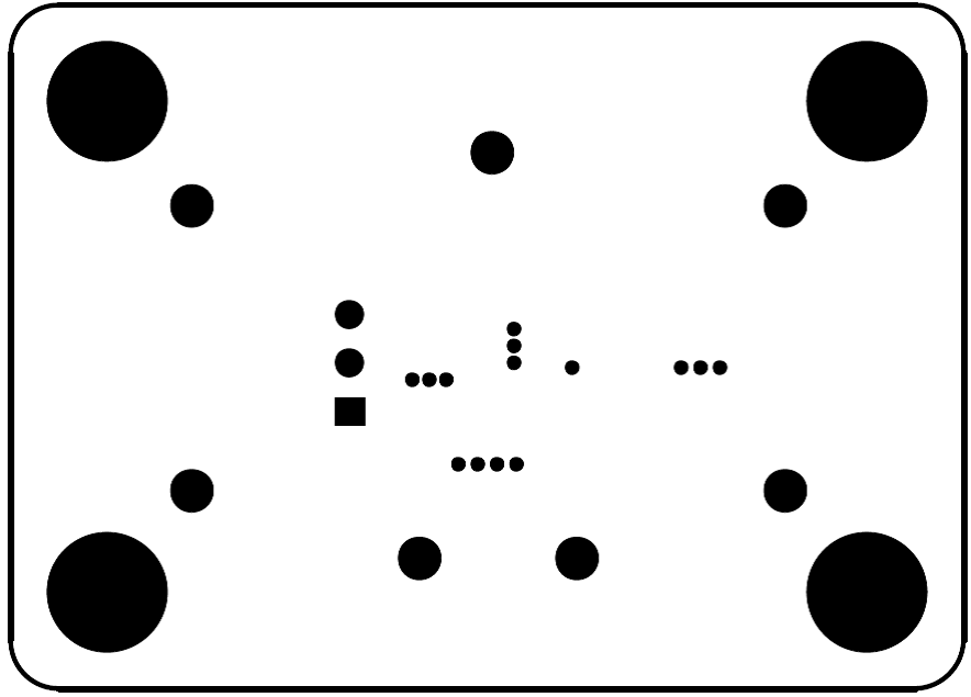
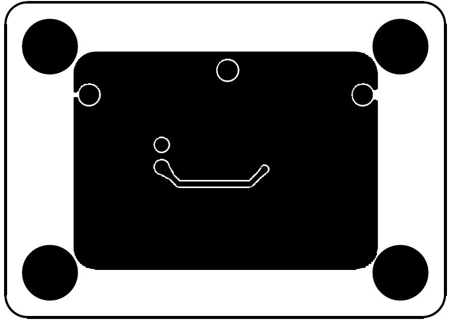
EVB Layout
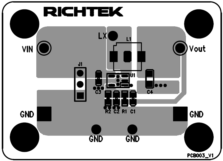
Top View (1stlayer)
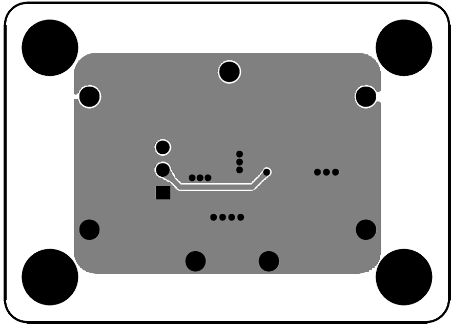
Bottom View (2nd Layer)
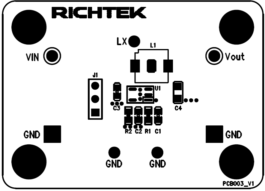
Component Placement Guide—Component Side (1stlayer)
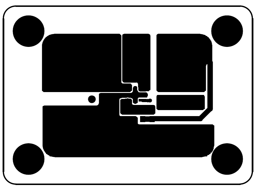
PCB Layout—Component Side (1stLayer)
Component Placement Guide—Bottom Side (2nd Layer)
PCB Layout—Bottom Side (2nd layer)